| Home | [an error occurred while processing this directive]History | [an error occurred while processing this directive]RAMBOard 2/C | [an error occurred while processing this directive]1571 RAMBOard | [an error occurred while processing this directive]RAMBOard (std.) |
|---|---|---|---|---|
| [an error occurred while processing this directive] | Speed Control | [an error occurred while processing this directive][an error occurred while processing this directive] | [an error occurred while processing this directive] | References |
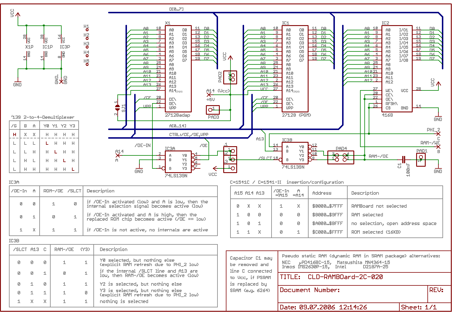
CLD's RAMBOard, revision 2/C
The reason, why the original author of the newsgroup discussion (see History section) asked for help to identify some piece of hardware was, that he didn't have any clue how to correctly install that hardware. The main problem was, that his revision of the RAMBOard differed to others, that were more common.

To make use of the RAMBOard, it not only needed to be inserted into a freed up socket of the Commodore disk drive, but three additional wires had to be connected elsewhere. The main board had to be plugged into the ROM socket of the 1541 disk drive by removing the ROM from the socket and placing it into a socket on the extension board. Because the board got a 28pin socket adaptor, it was relatively clear at the beginning of the discussion, that his RAMBOard revision most probably must be a version for the Commodore 1541C or 1541-II floppy disk drive.
With the help of some pictures from the scanned hardware, later measurements and a lot analyses, the schematic of his hardware could be reengineered (see the picture to the right).
Identifying the RAM chip
There have been some oddities left after the first schematic was done. The RAM chip, which was assumed a standard 6264 static RAM (SRAM) type at first, contained some useless connections. Pin 1 was connected in parallel to pin 26, but pin 1 is always marked as not connected (N.C.) in all the 6264 and compatibles datasheets. And then there is a capacitor connected to the chip/output enable line that doesn't make any sense.
Moreover, on his way to identify the hardware parts and the controlling logic on his own, the originating author and others of one of the newsgroup discussions stumbled over the very uncommon RAM chip type IMS2630P that was used on his board and a D2187A on another. Since no one seemed to be able to correctly identify the exact funtion of these chip types some questions remained open.
Months later, after the whole newsgroups discussion was over, I got into contact to people from the former producer/manufacturer CLD (please don't ask me for that contact, the persons behind CLD desperately want to stay private). From this contact I got very useful informations and especially some hints about the RAMs that were used in most of their RAMBOard hardware extensions.
Pseudo static RAM
Actually pseudo static RAM (PSRAM) is of DRAM type (dynamic RAM), but it is packaged just the same as common SRAM chips (static RAM). In the late 1980'ties it was called iRAM. The big advantage of using PSRAM instead of SRAM was its very low price (1 USD instead of 30 USD in the year 1989). The disadvantage was that PSRAM needs to be refreshed just like DRAM and that is, what pin 1 is used for. As I found out in an old chip comparison chart (PDF file, 93KB), the PSRAM chip does its refresh cycle, whenever pin 1 is pulled to low level.
To accommodate the RAMBOard circuit to the PSRAM chip type, CLD used the processor signal Φ2. Whenever Φ2 is low, the RAM chip does its refresh cycle, if Φ2 goes high, the RAM can be accessed normally. But the chip/output enable line (/CE, /OE) needs to be deferred a little bit after each refresh cycle, therefore the additional capacitor is used. It delays the falling edge of the /OE signal by some nanoseconds, so that the PSRAM is out of its refresh cycle for sure.
As the schematic was created and proofed for consistency with the original hardware and with the additional information about the circuitry for the PSRAM chip type, it is relatively easy to determine, where the three free wires named »A«, »B« and »C« have to be connected to:
-
RAM- or ROM-Enable selection, this wire should be connected to
the address line A14 (6502 processor, pin 24).
-
RAM-Write-Enable, this wire should be connected to the RAM-/WE
signal of the builtin RAM chip of the disk drive (pin 21 of the
2016 RAM chip).
- PSRAM refresh signal, this wire should be connected to the Φ2 system clock signal (6202 processor, pin 39). If the RAMBOard doesn't make use of a PSRAM chip type but a standard SRAM (e.g. 6264), then line »C« could be connected to a static high level so that the second chip select signal gets active all the time. Furthermore the capacitor could be removed, but these two modifications are not neccessary, if the RAM chip is fast enough whoch SRAMs mostly are.
Documentation
What the printed manual says
Some years later again another thread about CLD's RAMBOard raised. This time a user provided scans of the »official« installation manual for the RAMBOard 2/C, which then got converted to ASCII text, retypesetted and put into a PDF file; content and appearance of the manual could be preserved in 100% true electronic form.
The official installation manual advises the user to connect the three wires denoted A, B and C to:
-
RAM- or ROM-Enable selection, this wire should be connected to
the address line A14 (6502 processor, pin 24, location U3).
-
RAM-Write-Enable, connect this wire to pin 22 of one of the both
VIA 6522 chips (location U6).
-
Φ2 system clock signal, used as PSRAM refresh, connect this
wire to pin 25 of the other VIA 6522 chip (location U8).
Interestingly this manual mentions a) another »1541 II RAMBOard V2« and b) it got a memo taped on page 3 from the distributor SSI that contains a note from »Dan«.
-
1541 II RAMBOard Installation (PDF-Version, english,
173KB),
converted to eText and recompositioned to match the original as
far as possible.
-
1541 II RAMBOard Installation (ASCII-Version, english,
14KB),
eText, as contributed to
Project64,
look it up at the
Commodore
Peripheral Documents section.
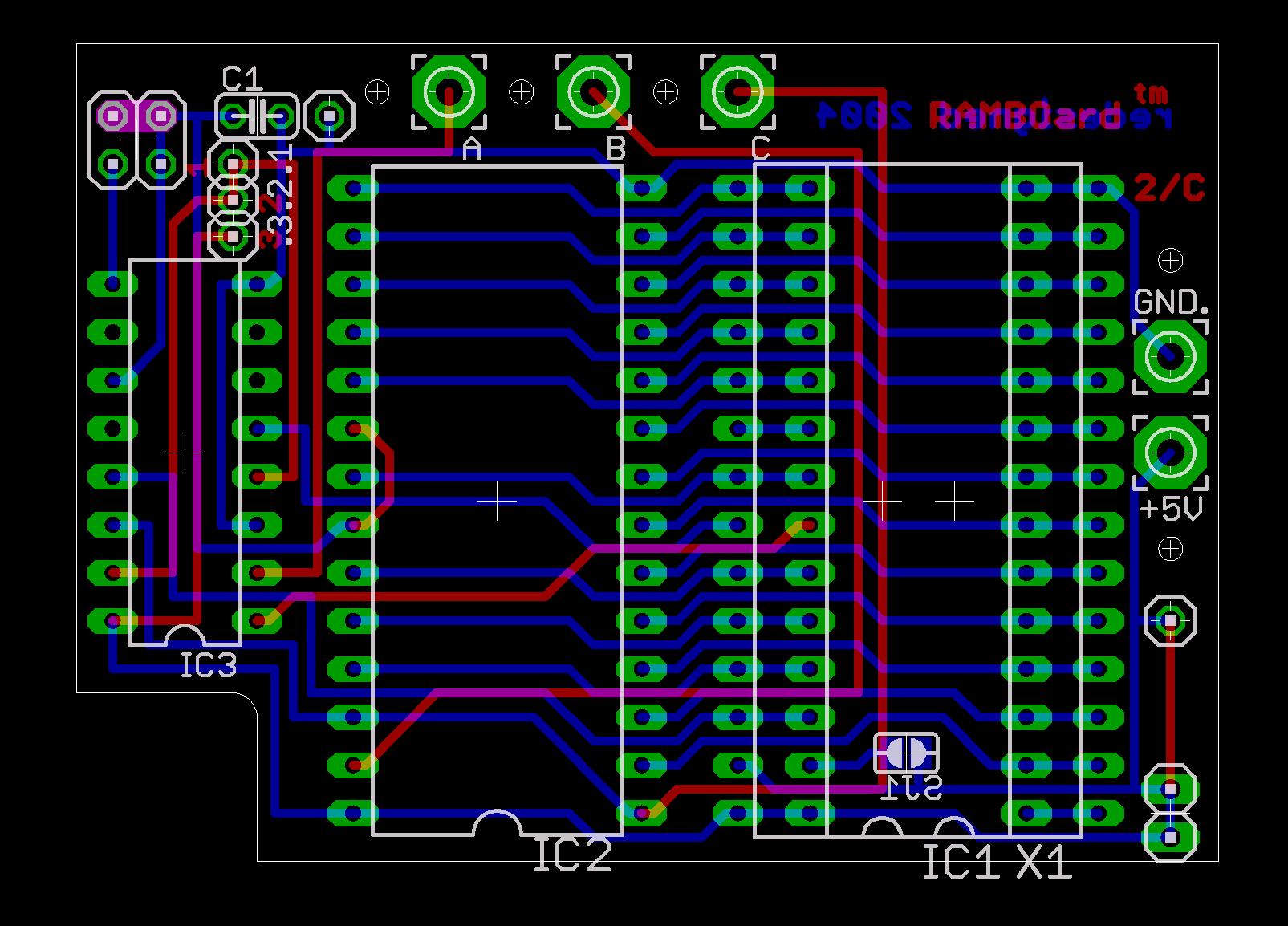
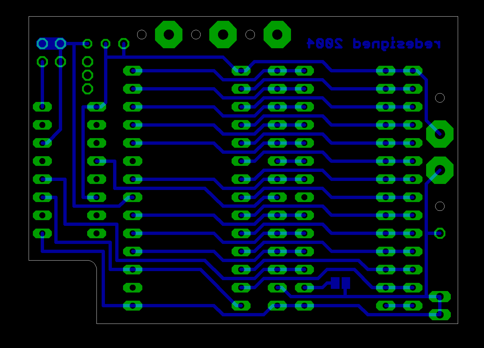
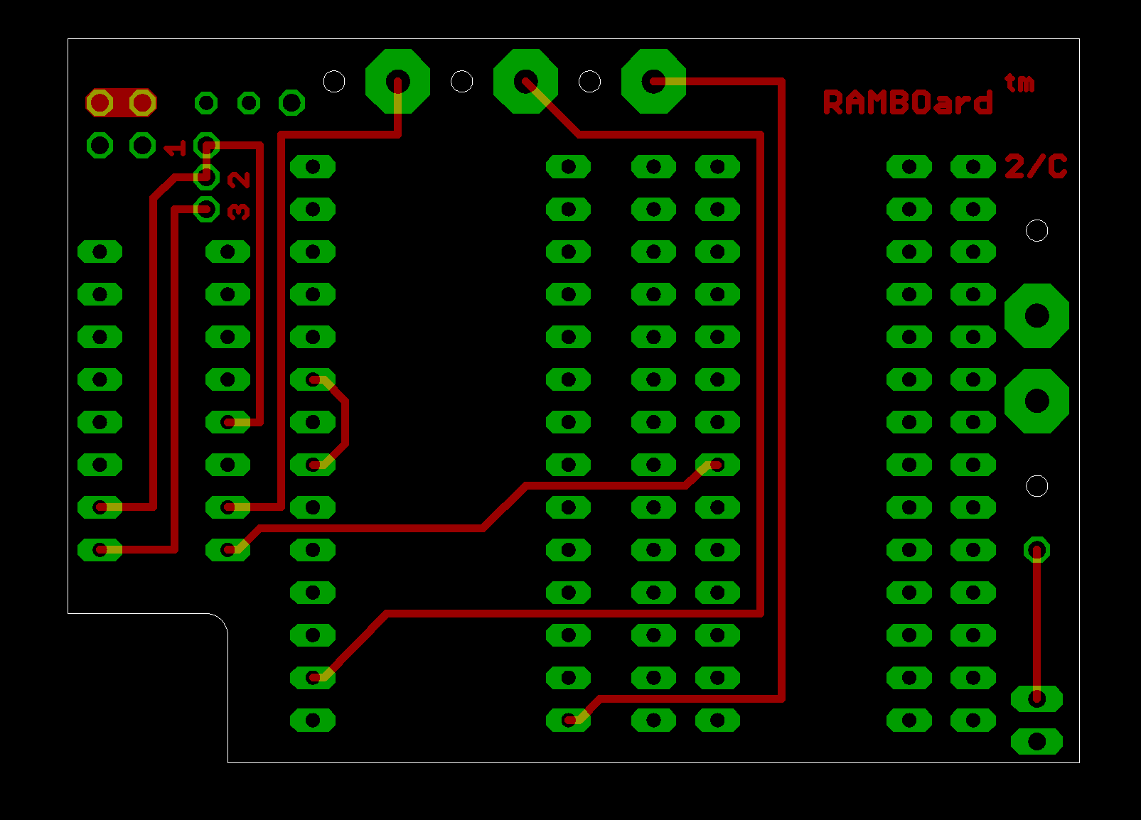
Redesigned board layouts of CLD's RAMBOard 2/C
By creating the schematic the board layout was done also. It was a lot easier to check for consistency errors with the original board layout that way. This section lists all additional documents that were created through the reengineering process. Take note that the layout software source files (CadSoft Eagle freeware version 4.1) are not available for download here, because I don't want to help others in making pirated copies from this hardware. I don't have an official agreement with the former manufacturer CLD and therefore the purpose of this site is limited to helping people to understand, how this hardware does work.


| Bill of materials | |||
|---|---|---|---|
| X1 | - | 28pol. precision socket adaptor, connects to the 1541C/1541-II drive DOS ROM socket | |
| IC1 | - | 27128 EPROM, the drive DOS ROM that has been pulled out of its socket from the drive | |
| IC2 | - | 4168 pseudo static RAM 8Kx8 (alt. 6264 static RAM) | |
| IC3 | - | 74LS139 | |
| C1 | - | 100nF ceramic capacitor | |
Schematic and board layout in print production resolutions
PDF-File of the reengineered version 0.20 of the schematic and layouts of CLD's RAMBOard, revision 2/C