| Home | [an error occurred while processing this directive]The Hardware | [an error occurred while processing this directive]Versions | [an error occurred while processing this directive]Documents | [an error occurred while processing this directive]Protected Area |
|---|
|
||||||||
Page jump links:
Heading
PCB Connections
The parts listing
The schematic
Address deconding based on the PROM 82S123A (aka 74S188)
Functional description of the drive expansion board
Downloads
Description of the electronics of the Floppy-Speeder Professional-DOS, Version 1
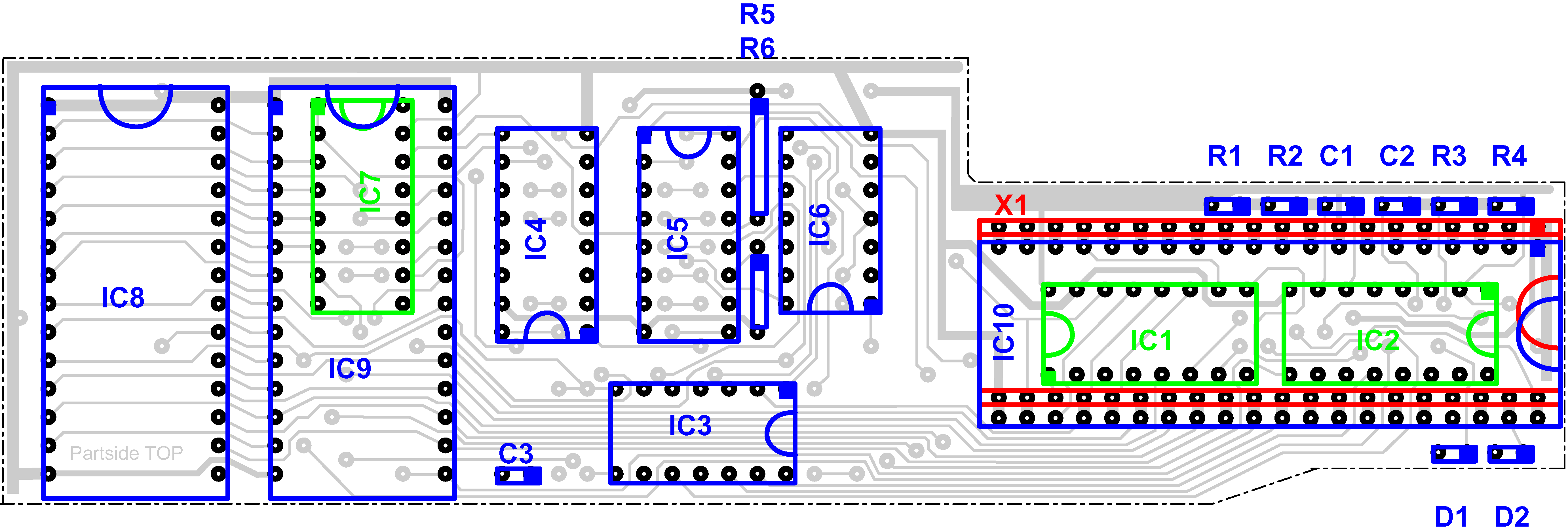
For all further descriptions the following parts placement and numbering is used. It shows the Professional-DOS drive expansion board PCB from the top side (parts side):
|
|

150 dpi version of this picture, 1382x467, 28kB 600 dpi version of this picture, 5529x1869, 159kB |
Pin 1 of all components is marked with a little square (♦, not really :-). In case of the diodes (D1 and D2), pin 1 marks the cathode, in the case of C3 it marks the plus connection. In case of the resistors (Rx) and capacitors (C1 and C2), pin 1 is only marked for the use with the crossconnection table below.
PCB Connections
The first step in revealing the exact working of Professional-DOS Version 1 was to find out which of the ICs was connected to each other and how. The result was a crossconnection table, that cannot be presented with plain HTML code. It's simply too big, to watch it with a simple WWW-Browser, so get it as a PDF-File (11kB) and print it to a DIN-A3 paper if possible.
This table may be (a little bit :-) confusioning for the non-technician-eye. Well, each row represents a line of two or more pins that are connected to each other. The first three columns tell you what pin of which part was tested against each other (first measurement point) and additionally labels the whole line (e.g. Vcc, GND or A13). The rest of the row tells, which pins of the other parts are connected to the first one, if any. Because the first measurement point is also listed in the right half of the table, there's always at least one connection (each pin is connected to itself, of course).
The parts listing
With the crossconnection table, a prototype board, some helper TTL circuits, an electronic table of all TTL ICs and some days of work all the IC labels could be identified and proofed. These parts are listed in the following table.
| Label | Description |
|---|---|
| R1, R4 | Resistor, 1K5 ± 1% |
| R2, R3 | Resistor, 9K1 ± 1% |
| R5, R6 | Resistor, 1K8 ± 1% |
| C1, C2 | Capacitor, 56 pF |
| C3 | Capacitor, Tantal, 10 µF/16V (added later for better stability) |
| D1, D2 | Diode, 1N4148 |
| IC3 | 74LS00, directly mounted onto the PCB |
| IC4 | 74LS157, directly mounted onto the PCB |
| IC5 | 74LS367 , directly mounted onto the PCB |
| IC6 | 74LS74, directly mounted onto the PCB |
| IC8 | EPROM, 27128, placed into a socket |
| IC9 | Static RAM CMOS 8192x8, TC5565PL-15 or similar (6164, 6264LP-10, ...), placed into a socket |
| IC10 | empty socket, 40 pin (reserved for 6502 processor) |
| IC1 | 82S123A (aka. 74S188), mounted below IC10 |
| IC2 | 74LS123, mounted below IC10 |
| IC7 | 74LS173, mounted below IC9 which has to be placed into a socket |
| X1 | IC adaptor, 40 pin, soldered onto the bottom side of the PCB |
The schematic
With the informations collected until here, it was no problem anymore to create a full featured schematic of Professional-DOS Version 1.
|
|
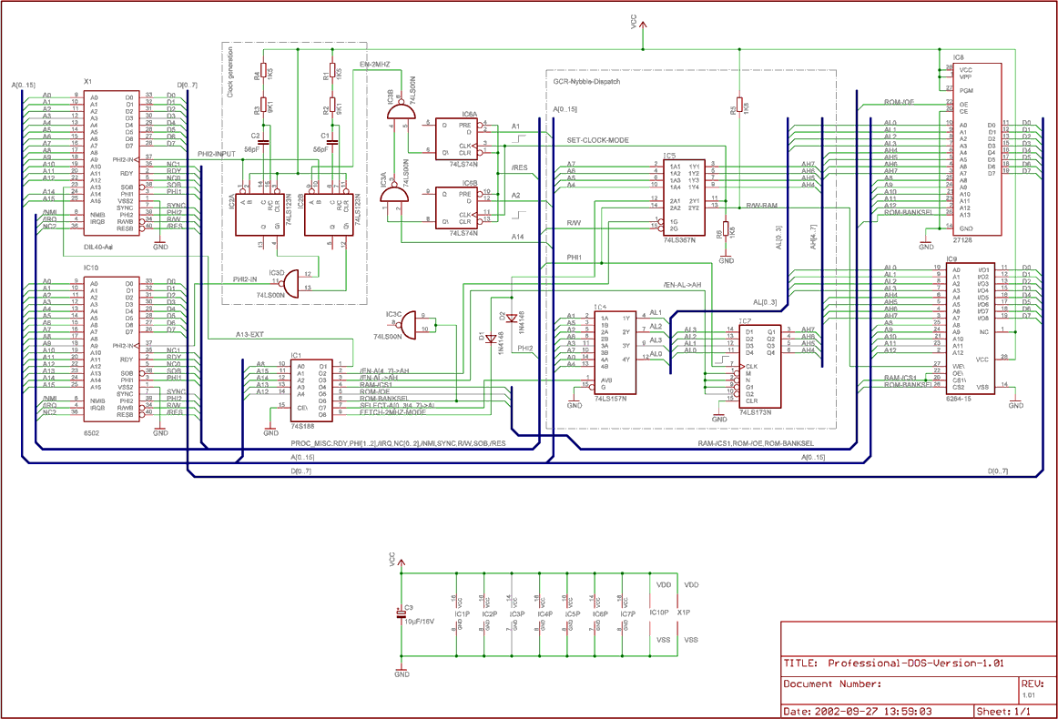
75 dpi version of this picture, 1162x790, 55kB 600 dpi PDF file of this schematic (DIN-A3 landscape), 251kB You can find the source version in Eagle-Format at the bottom of this page |
It shows the 2MHz clock generator logic, some FlipFlops for switching the clock generator into different modes, an address decoder based on a simple 32x8Bit-PROM and the GCR nibble codec (the hardware part of it).
Address decoding based on the PROM 82S123A (aka 74S188)
Reading out the contents of the PROM was not very difficult but time consuming. In a first step this job was done manually. Because of some difficulties with interpreting the results, the PROM was read out again with a little helper hardware for the C64 (CIA 6526 added to the expansion port) and some lines of BASIC. These new results didn't differ, so the PROM readout is double checked now.
Since this chip contains 5 independent inputs, 32 different bit combinations had to be tested through. Each input bit pattern produces an 8-Bit output combination. Please view the result tables and explanations as PDF version (12kB) or from this text file, because the following table can you only give a short functional decoding overview:
| IC1: selected address |
progr. byte |
6502 processor selected address space | external address simulation |
internal RAM/ROM enabling | special functions |
|---|---|---|---|---|---|
| 0 | 61 | 0x0xxx | 0x2xxx | ||
| 1 | 61 | ||||
| 16 | 61 | 0x1xxx | 0x3xxx | ||
| 17 | 61 | ||||
| 8 | 61 | 0x2xxx | |||
| 9 | 61 | ||||
| 24 | 61 | 0x3xxx | |||
| 25 | 61 | ||||
| 4 | 61 | 0x4xxx | 0x6xxx | ||
| 5 | 61 | ||||
| 20 | 61 | 0x5xxx | 0x7xxx | ||
| 21 | 61 | ||||
| 12 | 61 | 0x6xxx | |||
| 13 | 61 | ||||
| 28 | 61 | 0x7xxx | |||
| 29 | 61 | ||||
| 2 | 43 | 0x80xx, 0x82xx, ... | 0xAxxx | HI-ROM (GCR tables) | GCR codec LO mode |
| 3 | 107 | 0x81xx, 0x83xx, ... | GCR codec HI mode | ||
| 18 | 45 | 0x9xxx | 0xBxxx | HI-ROM (P.DOS ext.) | |
| 19 | 45 | ||||
| 10 | 53 | 0xAxxx | RAM | ||
| 11 | 53 | ||||
| 26 | 53 | 0xBxxx | |||
| 27 | 53 | ||||
| 6 | 60 | 0xCxxx | |||
| 7 | 60 | ||||
| 22 | 60 | 0xDxxx | |||
| 23 | 60 | ||||
| 14 | 13 | 0xExxx | LO-ROM (P.DOS) | ||
| 15 | 13 | ||||
| 30 | 13 | 0xF0xx, 0xF2xx, ... | |||
| 31 | 141 | 0xF1xx, 0xF3xx, ... | set clock mode |
Functional description of the drive expansion board
IC1, dual retriggerable monostable multivibrator, is responsible for the 2 MHz clock generation of the drive expansion board. One of the monoflops is triggered with the negative edge of the clock input signal Φ2, the other one with the positive edge. The discretes set up a pulse width of nearly ∼250ns for each of the monoflops. Combining the both inverted outputs /Q with a NAND gate results in a fine 2 MHz clock.
Additionally the pulse generation of one of the monovibrators can be controlled externally. This way the clock generation can be switched between 1 MHz and 2 MHz mode. In 1 MHz mode the resulting duty cycle is not fifty-fifty of course.
The 2 MHz mode enabling line comes from the Flip-Flops (IC6, using the inverted outputs /Q) and some NAND gate logic combining the Flip-Flop outputs with the address line A14. If Flip-Flop (FF) A (D input is A1) is set, always 1 MHz mode is enabled. I FF A is not set, but FF B (D input is A2) is set always the 2 MHz mode is active. If both Flip-Flops are not set (the inverted /Q output is 1 on both), the 2 MHz operation depends on the address line A14. If A14 is high, 1 Mhz is selected, if it is low, then the 2 MHz mode is enabled. This state could be called »automatic clock mode«
But how can the Flip-Flops be set? The controlling clock line is coming from the address decoder, that is explained in the section above. But there are some circuits in between, that are possibly somewhat uncommon in their use. Let's simply make a little truth table with the parts D1, D2, IC5 and R6:
| R/W | Φ2 | EN-2MHz (from IC1) |
after D1/D2 |
after IC5 pin 11 |
IC5/11 with R6 |
|
|---|---|---|---|---|---|---|
| 0 | 0 | 0 | 0 | 0 | 0 | |
| 0 | 0 | 1 | 0 | 0 | 0 | |
| 0 | 1 | 0 | 0 | 0 | 0 | |
| 0 | 1 | 1 | 1 | 1 | 1 | |
| 1 | 0 | 0 | 0 | Z | 0 | |
| 1 | 0 | 1 | 0 | Z | 0 | |
| 1 | 1 | 0 | 0 | Z | 0 | |
| 1 | 1 | 1 | 1 | Z | 0 |
You can see, that only when the processor is in write mode (R/W=0) and Φ2 and EN-2MHz are high then the result is a high. With the rising edge of this high, the both Flip-Flops store the current state of the address lines A1 and A2. By accessing (writing) different addresses in the ROM area of 0xF1xx, 0xF3xx, ..., 0xFFxx (see address decoder), the desired clock mode can be set.
The same goes with IC5, pins 13, 14, 15 and R5 (signals: R/W and Φ1). Make a little truth table of it and you'll probably realise, that this is a standard circuit for setting up correct /Write signals (/Read and /Write separated) for »CBM incompatible« parts. You can see similar circuitries in every CBM computer for setting up read and write signals for typical ROMs and static RAMs.
The heart of the Professional-DOS expansion board is surely the »GCR nibble dispatcher«, built with the parts IC4, IC5 and IC7. It mainly maps the 6502 address lines A0 to A7 to two internal busses named AL[0..3] and AH[4..7] where the EPROM and RAM are connected to. In normal operation the bus A[0..7] is mapped straight through to AL and AH just like the RAM and ROM were directly connected to the 6502.
Always when the address space 0x8xxx is selected, the address decoder enables the nibble codec (switch IC5 off and IC7 on). The main interesting thing on it is IC7, a 4-Bit D register. It could be named as a one-stage-4-Bit-queue, because it gives out the last stored 4-Bit-AL-value to the AH bus and stores the current AL bus state. The current AL value is selected with IC4 and it can be either A[0..3] or A[4..7] depending on the selected 6502 address (see address decoder). With this circuitry it is possible to »shift« 4-Bit nibbles. With additional EPROM page selecting done in software, it simplifies GCR decoding of a whole 5-Byte GCR group a lot since there is no bit shifting needed anymore.
Once Andreas Boose said in »Re: Can you identify this fastload HW?« :
»Professional DOS is not 'decoding the original GCR-code by hardware'.«
Yes, partly, he meant, that not all of the decoding process is fully done in hardware. The processor e.g. has to select the right Codec table and to use indexed adressing schemes. On the other hand you can see here, that it surely wouldn't work without some special circuits. As a conclusion, this GCR-Codec (Encoder/Decoder) could be called as an ideal symbiosis between hard- and software.
Downloads
-
Professional-DOS schematic (54kB)
-
ZIP-File with the schematic of Professional-DOS Version 1
in Eagle
(Freeware Light Edition)
source format.
-
Professional-DOS PCB-Layout (260kB)
-
PDF file containing the reconstructed PCB-Layout of the
Professional-DOS drive expansion board. The Layout is not
100% identical to the original PCB, because of some non
standard pin widths. It is not meant for reproduction of
Professional-DOS (it was drawn using MS-Powerpoint), but
should only be a better representation of the PCB photos
in the picture gallery.
-
Professional-DOS V1 electronics collection(117kB)
- This ZIP archive contains the crossconnection table, the both files with the PROM content descriptions and a modified version of this website (bigger contents were removed).
Page jump links:
Heading
PCB Connections
The parts listing
The schematic
Address deconding based on the PROM 82S123A (aka 74S188)
Functional description of the drive expansion board
Downloads